Commercial Micro Manufacturing - November 2024
Supporting Sub-Angstrom Materials Research at Oak Ridge National Laboratory
ORNL’s Center for Nanophase Materials Sciences utilizes Scanning Transmission Electron Microscopy to analyze atoms in individual nanostructures, permitting the atomic structure of materials to be seen more clearly at atomic dimensions of smaller than one ten-billionth of a meter. Critical to this sub-angstrom research is Negative-Stiffness vibration isolation.
by Jim McMahon
Advancements in nanofabrication, pharmaceuticals, energy and aerospace follow breakthroughs in the understanding of materials. These breakthroughs unlock unique functionalities that create new pathways to design future devices.
The Center for Nanophase Materials Sciences (CNMS) at Oak Ridge National Laboratory (ORNL) is at the forefront of one of the most powerful capabilities for exploring the nature of materials and energy. CNMS emphasizes discovery of new materials, and the understanding of underlying physical and chemical interactions that enable the creation of nanomaterials.
The center is unique in that it provides a platform for a vibrant national and international research community that brings together ORNL research staff, technical support staff, students, postdoctoral fellows and collaborating guest scientists, accommodating both short-term and long-term collaborative research projects.
To support this impressive research capability, CNMS researchers have access to state-of-the-art microscopy instruments in its Advanced Microscopy Laboratory (AML) for a broad range of nanoscience research, including nanomaterials synthesis, nanofabrication, imaging/microscopy/characterization, and theory/modeling/simulation.
Amongst the instruments used for materials research in the ALM are some of the most advanced Transmission Electron Microscopes (TEM) and Scanning Transmission Electron Microscopes (STEM). Transmission Electron Microscopy
TEMs utilize a technique in which a beam of electrons is transmitted through an ultra-thin specimen, interacting with the specimen as it passes through. An image is formed from the interaction of the electrons transmitted through the specimen. The image is magnified and focused onto an imaging device, such as a fluorescent screen, a layer of photographic film, or to be detected by a sensor such as a CCD camera. TEMs use phase-contrast, and therefore, produce results which need interpretation by simulation.
The ability of electron microscopes to analyze atoms in individual nanostructures has been limited by lens aberrations, but advances in aberration-correcting optics have led to greatly enhanced instrument performance and enabled new techniques in electron microscopy.
Correction of spherical aberration in the Transmission Electron Microscope, for example, has allowed routine sub-angstrom resolution imaging. Higher resolution greatly improves sensitivity to single atoms – either lying on a material’s surface or inside the bulk – permitting the atomic structure of materials to be seen more clearly, and allowing light elements to be seen in the presence of heavy atoms. Aberration correctors have enabled electron probes with sub-angstrom diameters to be used, making it possible to identify individual atom columns with unprecedented clarity.
Scanning Transmission Electron Microscopy
A type of TEM which has become highly appealing, the STEM, also permits the electrons to pass through an ultra-thin specimen, however, the STEM focuses the electron beam into a narrow spot which is scanned over the sample in a raster. The rastering of the beam across the sample makes the STEM suitable for analysis techniques, such as mapping, where the signals can be obtained simultaneously, allowing direct correlation of image and quantitative data.
By using a STEM equipped with a high-angle detector, it is possible to form atomic resolution images where the contrast is directly related to the atomic number (Z-contrast image). The directly interpretable Z-contrast image makes STEM imaging with a high-angle detector preferable to TEM in some applications. For example, oxygen can now be visualized in superconductors and colossal magnetoresistant manganites where it plays a dominant role in determining properties.
Electron energy loss spectroscopy (EELS) is a STEM measurement technique made possible with the adaption of an electron spectrometer. With the addition of EELS, elemental identification is possible, as well as additional capabilities of determining electronic structure or chemical bonding of atomic columns. With EELS, the STEM does not just produce an image, it can also do chemical mapping. Instead of just detecting what scatters from the atom, it can show changes in chemical balance and see an incredible amount of detail about the physics interface when two different materials come together.
“We are using the STEM for different applications,” said Dr. Andrew R. Lupini, R&D staff member in the Center for Nanophase Materials Sciences at Oak Ridge National Laboratory in Tennessee. “As well as the imaging, this STEM can do very high-energy resolution spectroscopy. For example, we can probe properties of materials relating to their bonding and measure their temperature on a very local scale.”
With correction of spherical aberration, the STEM can resolve more than just seeing the atoms more clearly. The high-energy convergent electron beam in STEM provides local information of the sample, even down to atomic dimensions of smaller than one ten-billionth of a meter.
CNMS’ latest STEM pushes the spatial, temporal, and energy resolution limits for imaging and spectroscopy. The Nion Hermes STEM-EELS is a next-generation low-voltage (60-100kV) 𝛼-monochromated 5th-order, aberration-corrected (MAC)-STEM.
CNMS’ Nion Hermes STEM-EELS enables access to excitations of phonons, molecular vibrations, and other mid-infrared quasiparticles, and is capable of energy resolution for low-loss EELS while retaining sub-angstrom spatial resolution to 0.1 nm maximum.
STEM Sensitivity to Vibration
Scanning Transmission Electron Microscopes are more sensitive to ambient conditions, with the addition of field emission guns, imaging filters, and spherical aberration correctors that give higher spatial and energy resolution, and EELS.
The ultimate performance of these extremely sensitive microscopes is strongly influenced by factors such as magnetic fields, barometric pressure changes, room- and chilled-water temperature variations, grounding problems, and quite significantly by floor and acoustic vibrations.
Vibration can reach the STEM through the floor from movement of outside vehicle traffic, elevators, HVAC systems, building pumps and motors, and ancillary equipment providing support to the microscope. Both vertical and horizontal vibration will negatively influence the focus and resolution of the image being viewed.
“With the Nion Hermes STEM-EELS, we can see single atoms, so any vibration makes the resolution worse or difficult to see,” explained Dr. Lipini.
Atomic resolution spectroscopy is particularly sensitive to environmental instabilities as a result of its long acquisition times. The serial nature of the image acquisition in STEM makes the instabilities appear as image distortions. STEMs are most sensitive to low frequency vibration, in the range of a few Hertz. These vibrations are challenging to eliminate from the microscope’s environment.
Negative-Stiffness Vibration Isolation
Because of its high vibration isolation efficiencies, particularly in the low hertz frequencies, Negative-Stiffness vibration isolation was selected by ORNL’s Center for Nanophase Materials Sciences for sub-angstrom materials research with its Nion Hermes STEM-EELS.
“Our Nion Hermes STEM-EELS site is equipped with field-cancellation devices to cancel out magnetic fields,” added Dr. Lipini. “We have it located in a soundproof room using sound dampening materials to negate the impact of sound. But we still needed to isolate the low frequency vibrations transmitting through the floor. For that we chose Minus K Technology’s Negative-Stiffness vibration isolators.”
Introduced in the mid-1990s by Minus K Technology, Negative-Stiffness vibration isolation has been widely accepted for vibration-critical applications, largely because of its ability to effectively isolate lower frequencies, both vertically and horizontally.
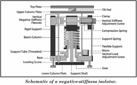
Negative-Stiffness isolators are unique in that they operate purely in a passive mechanical mode. They do not require electricity or compressed air. There are no motors, pumps or chambers, and no maintenance because there is nothing to wear out.
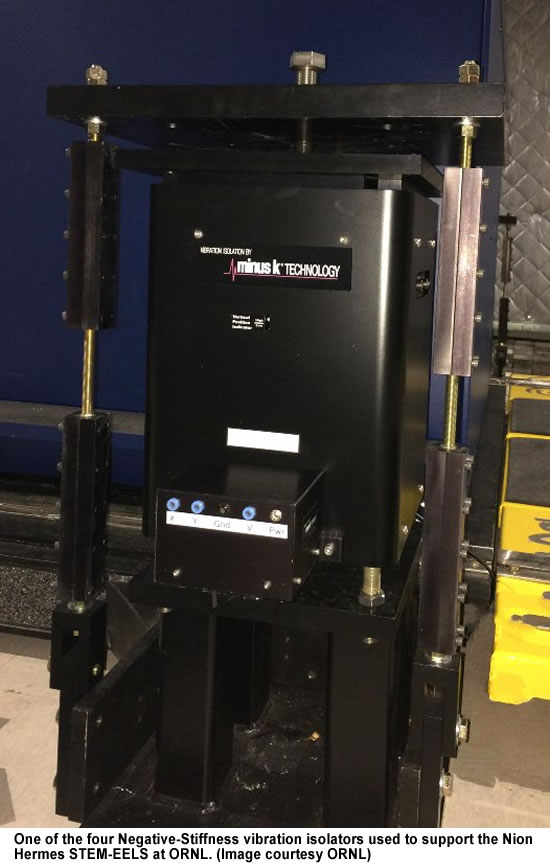
“Vertical-motion isolation is provided by a stiff spring that supports a weight load, combined with a Negative-Stiffness mechanism,” said Erik Runge, Vice President of Engineering at Minus K. “The net vertical stiffness is made very low without affecting the static load-supporting capability of the spring. Beam-columns connected in series with the vertical-motion isolator provide horizontal-motion isolation. A beam-column behaves as a spring combined with a negative-stiffness mechanism. The result is a compact passive isolator capable of very low vertical and horizontal natural frequencies and high internal structural frequencies.”

Negative-Stiffness isolators achieve a high level of isolation in multiple directions, with the flexibility of custom-tailoring resonant frequencies to 0.5 Hz vertically and horizontally (with some versions at 1.5 Hz horizontally)*. When adjusted to 0.5 Hz, the isolators achieve approximately 93 percent isolation efficiency at 2 Hz, 99 percent at 5 Hz, and 99.7 percent at 10 Hz.
(*Note that for an isolation system with a 0.5 Hz natural frequency, isolation begins at 0.7 Hz and improves with increase in the vibration frequency. The natural frequency is more commonly used to describe the system performance.)

Preferred Vibration Isolation for Sub-Angstrom Research
Selecting the most optimum vibration isolation system is critical when dealing in sub-angstrom measurements. Air tables have always been weak with isolating low-frequency vibrations below 5 hertz, precisely the vibrations that are most disruptive to sub-angstrom recordings.
Electronic-force cancellation systems, also called active vibration isolation, use electronics to sense motion, then add forces electronically to cancel out or prevent the vibrations. Active systems have limited dynamic range. Vibrations that are too large can cause the system to go into positive feedback. Vibrations that are too small may not even be detected. Not ideal for atomic-scale microscopy.
For this application, four Negative-Stiffness isolators were employed, one for each corner supporting the platform upon which rests the Nion Hermes STEM-EELS.
“Vibration isolation that has an active control mechanism is very difficult to maintain under changing conditions,” said Dr. Lupini. “Passive isolation is running all the time, so if you have a power cut, or some other change or interruption, it still performs.”
Negative-Stiffness vibration isolation has become a preferred system to analyze atoms in individual nanostructures, permitting the atomic structure of materials to be seen more clearly at sub-atomic levels.
About Dr. Andrew R. Lupini
Dr. Lupini obtained his Ph.D. in Physics from the Cavendish Laboratory of Cambridge University in the UK in 2001. Dr. Lupini is one of the inventors of the first aberration-corrector in a scanning transmission electron microscope to demonstrate an improved resolution. He is currently a R&D staff member in the Center for Nanophase Materials Sciences at Oak Ridge National Laboratory in Tennessee. His research interests include all forms of electron microscopy and spectroscopy, especially as applied to new or quantum materials.
About the Center for Nanophase Materials Sciences, Oak Ridge National Laboratory
The Center for Nanophase Materials Sciences (CNMS) is part of Oak Ridge National Laboratory (ORNL), a national multi-program research and development facility of the U.S. Department of Energy. CNMS offers the national and international user community access to staff expertise and state-of-the-art equipment for a broad range of nanoscience research, including nanomaterials synthesis, nanofabrication, imaging/microscopy/characterization, and theory/modeling/simulation.
For more information, contact Dr. Andrew R. Lipini, Center for Nanophase Materials Sciences, Oak Ridge National Laboratory, 1 Bethel Valley Road, Oak Ridge, TN 37830; Phone 865-387-0288; email arl1000@ornl.gov; www.ornl.gov.
About Minus K Technology, Inc.
Minus K® Technology, Inc. was founded in 1993 to develop, manufacture and market state-of-the-art vibration isolation products based on the company’s patented Negative-Stiffness technology. Minus K products are used in a broad spectrum of applications including microscopy, nanotechnology, biological sciences, semiconductors, materials research, zero-g simulation of spacecraft, and high-end audio. The company is an OEM supplier to leading manufacturers of scanning probe microscopes, micro-hardness testers and other vibration-sensitive instruments and equipment. Minus K customers include private companies and more than 300 leading universities and government laboratories in 52 countries.
Jim McMahon writes on industrial, manufacturing and technology issues. His features have appeared in more than 3,500 business and trade publications worldwide.
|