![]()
Laser Focus World - October 2007
Vibration isolator from Minus K Technology is completely passive
By David L. Platus and David K. Ferry
With nanotechnology applications growing exponentially, scientists and engineers are putting their equipment in a multitude of locations where vibration noise is significantly high. Although big-budget installations (valued in the hundreds of thousands of dollars) typically incorporate adequate vibration isolation, many smaller-budget installations (those spending under $120,000 for equipment) do not-and these smaller sites represent the most rapid growth in the nanotechnology universe. It is estimated that 40% to 50% of smaller sites-in academia and industry-are initiated with inadequate vibration isolation.
![]() DAVID L. PLATUS is president and founder of Minus K Technology. 460 S. Hindry Ave. Unit C. Inglewood. CA 90301: e-mail: sales@minusk.com; www.minusk.com. DAVID K. FERRY is Regents' professor in the Nanostructures Research Group at Arizona State University. Center for Solid State Electronics Research. Box 875706, Tempe. AZ 85287; e-mail: ferry@asu.edu: www.fulton.asu.edu/-ferry/ferry.html.
DAVID L. PLATUS is president and founder of Minus K Technology. 460 S. Hindry Ave. Unit C. Inglewood. CA 90301: e-mail: sales@minusk.com; www.minusk.com. DAVID K. FERRY is Regents' professor in the Nanostructures Research Group at Arizona State University. Center for Solid State Electronics Research. Box 875706, Tempe. AZ 85287; e-mail: ferry@asu.edu: www.fulton.asu.edu/-ferry/ferry.html.
"When you get into the smaller instruments like white-light and laser interferometers, stylus profilers, and atomic-force microscopes (AFMs), then you have problems with site preparation," says George McMurtry, CEO of NanoAndMore (Lady's Island, SC), a distributor of AFM probes and nanotechnology peripherals. "In many cases, these instruments may be sitting on the fourth floor of a building and-without isolation-will end up getting really poor images."
Vibration-isolation options
Every building makes noise; the amount of noise depends on how high up off the ground you are and how old the building is. Within the building itself, vibrations can come from heating and ventilation system, fans, pumps that are not properly isolated, and elevators. External to the building, equipment can be influenced by vibrations from adjacent traffic, weather disturbances, construction, and other elements. These internal and external influences cause lower-frequency vibrations, which raise havoc with nano-instrumentation. For example, wind can cause a substantial resonance around 2 Hz. When trying to measure only very few angstroms or nanometers of displacement, any vibrations transferred into the mechanical structure of an instrument will cause vertical noise.
Since the 1960s, air tables have been used for isolation. Basically cans of air, they are still the most popular isolators. However, air tables with resonant frequencies at 2 to 2.5 Hz can typically only handle vibrations down to about 8 to 10 Hz-not quite low enough for optimum performance with modern nano-equipment. For purposes of clarity in
scanning-probe microscopes and interferometers, air tables are an inefficient isolation solution.
Isolators were used with AFMs in the 1980s, but the number of installed systems was small and most of them were in basements. Although some scientists are still suspending their very expensive AFMs from bungee cords hanging from the ceiling, many are not willing to take that risk any longer and have switched to alternative isolation systems.
 One type of system used is active isolation, also known as electronic force cancellation. Active isolation uses electronics to sense the motion, and then puts in equal amounts of motion electronically to compensate, effectively canceling out the motion. These systems can start isolating at frequencies as low as 0.7 Hz; quite sufficient for isolating the lower frequencies that are so damaging to image clarity with microscopes and interferometers. However, if mechanical isolation can be achieved without having to use energy, a scanning system will not be negatively influenced by problems of electronic dysfunctions and power modulations.
Negative-stiffness vibration isolation systems have become a growing choice for nanotechnology applications. Not only are they a highly workable vibration solution but they cost significantly less-up to one-third the price of active systems. These isolation systems enable vibration-sensitive instruments to operate in severe vibration environments, such as upper floors of buildings and clean rooms, and the images produced are significantly better than those achievable with pneumatic isolators.
Negative-stiffness isolation
Passive negative-stiffness isolators use a unique-and completely mechanical- concept in low-frequency vibration isolation. Vertical-motion isolation is provided by a stiff spring that supports a weight load, combined with a negative-stiffness mechanism (NSM). The net vertical stiffness is made very low without affecting the static load-supporting capability of the spring. Beam columns connected in series with the vertical-motion isolator provide horizontal-motion isolation. The horizontal stiffness of the beam columns is reduced by the "beam column" effect (a beam column behaves as a spring combined with an NSM). The result is a compact, passive isolator capable of very low vertical and horizontal natural frequencies and very high internal structural frequencies. The isolators (adjusted to 0.5 Hz) achieve 93% isolation efficiency at 2 Hz, 99% at 5 Hz, and 99.7% at 10 Hz.
"What negative-stiffness isolators provide is really quite unique to the field of nanotechnology," says Patrick O'Hara, president and CEO of Ambios Technology (Santa Cruz, CA), a manufacturer of microscopes, stylus profilers, and optical interferometers used in nanotechnology. "In particular, the transmissibility of a negative-stiffness isolator-that is, the vibration that transmits through the isolator as measured as a function of floor vibrations-is substantially improved over air or active isolation systems (sec Fig. 1). Although active isolation systems have fundamentally no resonance, their transmissibility does not roll off as fast as negative-stiffness isolators. So at building and seismic frequencies, the transmissibility of active isolators can be 10 times greater than negative-stiffness isolators. This causes substantial adverse measurement and imaging artifacts in the data. Air isolators have the added disadvantage that their 2 to 2.5 Hz resonance effects a significant loss in isolation capability below about 5 Hz."
Negative-stiffness isolators offer other advantages over air systems: they do not require an air supply or dedicated, large nitrogen tanks; the simple mechanical design mea ns there is nothing to wear out and no maintenance; performance can be achieved with compact benchtop isolators that conserve valuable laboratory space and are easily moved from one location to another; and they can be of an all-metal design and used in vacuum chambers and other adverse environments. Further, there are no dynamic-range limitations and no heat generation that can cause thermal drift.
<>
 AFM research
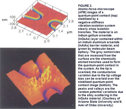
The Arizona State University (ASU; Tempe, AZ) Nanostructures Research Group team works on research in nanolithography and the physics of nanostructurcs and ultrasmall semiconductor devices. To study quantum dots, quantum wires, and ultrasmall semiconductor devices in a variety of materials, the group performs scanning-gate microscopy at low temperatures, a process that takes the equivalent of an AFM and puts a bias on it, allowing the study of the change in conductance of small semiconductor structures as this bias tip is moved around on a surface (see Fig. 2).
The system is mounted in a large cryogenic cooler maintained at about 300 mK, or 1000 times below room temperature. The AFM tip is on a cantilever that is metallized with a very thin layer of metal so that a voltage can be applied to it (a technique that was developed at Harvard four to five years ago). This voltage is used to perturb the structure being looked at. As the lip moves, it creates a voltage across the plane that is measured to determine certain electrical conductance through the overall system, as it is modified by the tip voltage. Although this type of experimentation is quite common, what is uncommon is that the team uses a negative-stiffness vibration-isolation system developed by Minus K Technology.
Any kind of vibration noise in the system makes the AFM cantilever tip move, and that gives bad signals and incorrect data. In this application, the team actually went further than most university applications by integrating a rather large magnet into the system. The magnet allows the researchers to look at different types of transport, such as the magneto transport of the semiconductors, a different mode of transport altogether.
The entire system had to be isolated, not just the cantilever. An extremely high level of vibration isolation was required because of the research parameters. Research using the system covers electron-beam lithography of quantum dots and quantum devices, with applications such as quantum ballistic transport at very low temperatures and high magnetic fields; magneto-transport studies used to probe the nature of electron dynamics in semiconductor quantum dots (which are quasi-zero-dimensional structures whose size is comparable to the Fermi wavelength of the electrons themselves); and surface chemical analysis performed with a scanning Auger microprobe That can achieve a lateral resolution of about 25 nm under good conditions.
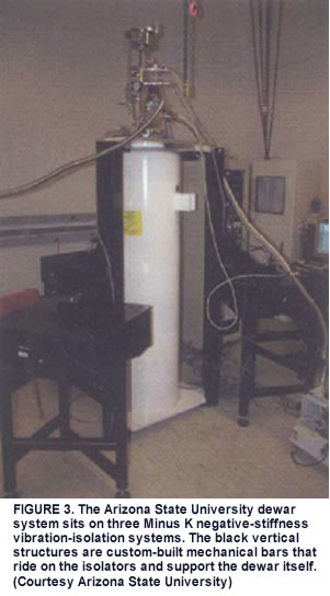
The negative-stiffness isolator is a passive isolation approach, and has a key advantage in that it requires no electricity. In a site where heat buildup could be an issue-such as with enclosed cryogenic chambers-negative stiffness becomes a highly efficient option to eradicate low-frequency vibrations. The ASU system uses three Minus K isolators to support the entire dewar system (see Fig. 3). During operation, of course, the pumps are disconnected to remove that source of vibration-the dewar and refrigerator system can hold the low-temperature environment for more than 40 hours, which allows a long experimental time at low vibration levels. The pumps can be reconnected to restore the low temperature and the process can be repeated as needed.
Today, leading technology transistors have critical dimensions below 25 nm, and the most critical dimension is the oxide thickness, which is 1 nm. In order to investigate these and smaller nanostructures with scanning-gate technology, the need for effective vibration isolation has never been greater and will continue to become more demanding as the nano industry progresses.