Photonics Online - July 2011
Negative-Stiffness Vibration Isolation Facilitates Growth Of Large Crystals For Field-Portable Gamma Ray Spectrometers
By Jim McMahon, Zebra Communications
Elimination of external vibrations plays a key role in
maintaining a stable growth process and maximizing the total
volume yield of very large crystals - destined for use in
homeland security field-portable applications for the detection
of gamma rays from special nuclear materials like plutonium
and highly enriched uranium.
At Kansas State University, a unique facility is dedicated
to the research and development of new and innovative
radiation detector technologies. The Semiconductor Materials
and Radiological Technologies (SMART) Laboratory is
the largest university-based radiation detection laboratory
in the country. It focuses on the detection of neutrons
and gamma-rays, primarily those from special nuclear
material (SNM) for homeland security applications. SMART
Lab investigates and fabricates a variety of detectors
which include compact low-power neutron detectors, high-resolution
room-temperature-operated semiconductor gamma ray spectrometers,
pixelated devices for gamma ray or neutron imaging,
and miniaturized gas-filled detectors. The laboratory
builds detectors from start to finish in readily deployable
packages for use in better securing our borders from
nuclear materials such as plutonium and uranium.
The gamma ray detection aspect of the laboratory's research
is focused on the discovery and development of new dense,
high-Z* semiconductor materials, such as cadmium zinc
telluride (CdZnTe or CZT) and mercuric iodide (HgI2),
and several scintillator materials including lanthanum
tribromide (LaBr3) and cerium tribromide (CeBr3). Research
conducted on large crystal growth with high-Z semiconductor
and scintillator materials has produced large crystal
ingot yields. (*The atomic number which uniquely identifies
a chemical element is represented by the symbol Z. Also
known as the proton number, it is the number of protons
found in the nucleus of an atom and identical to the
charge number of the nucleus.)
Gamma rays are electromagnetic radiation of high frequency
(very short wavelength), that are produced by sub-atomic
particle interactions such as electron-positron annihilation,
radioactive decay, fusion and fission. Gamma radiation is
highly penetrating photons, extremely energetic. To directly
detect them is very difficult, however - a material with
a high Z number is needed, representing a high number of
neutrons and protons in the nucleus. Those nuclei tend to
stop gamma rays much better than other elements such as
hydrogen or helium, for example. A crystal with a high-Z
number converts the gamma rays from electromagnetic waves
to excited electrons. The electrons move through the crystal
or create light, one or the other, and produce something
that is possible to be detected. If a crystal is very uniform,
very homogeneous - it can be determined that a gamma ray
interacted in the crystal by the effect that is observed
in it.
 Growing Giant Crystal
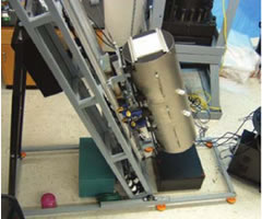
At the SMART Laboratory, crystals of CdZnTe
and the scintillator materials are grown via a vertical
Bridgman furnace. In this process, molten material is
directionally solidified from one end to the other to
produce a large-volume ingot that is a single crystal.
Methods to grow CdZnTe for gamma-ray spectrometers have
been explored since the early 1990s, yet a reliable
system to produce large crystals at an economical cost
has not been achieved until relatively recently.
Higher ingot yields enable smaller, faster and more
accurate sensors, and allow gamma-ray detectors to be
more economical and field-portable - benefits that can
have a significant impact on national security objectives.
Radiation detectors using CZT can operate in direct-conversion
(or photoconductive) mode at room temperature.
Essentially, SMART Lab researchers encapsulate the material
to be grown inside of a quartz ampoule under vacuum.
The quartz tube is put inside the furnace vertically
bringing the material to a molten state between 500°
- 1,100° C. Then they very slowly freeze the material
from bottom to top. If the thermal gradients are correctly
performed, a large crystal will develop. Once the crystal
is grown, it is extracted from the tube, trimmed to
size with a diamond wire saw and polished to produce
a detector.
Vibration Isolation
Critical to maximizing ingot yield is maintaining
a stable crystal growth process through the elimination
of external vibrations.
 "The general consensus within the crystal growth
community is that uncontrolled vibrations can destabilize
the growth interface," says Professor Mark Harrison
with SMART Lab. "As the material is freezing from
bottom to top, there is an interface between liquid
and solid, and it sets up a natural convection flow
that is ideal for growing a big, single crystal. If
a vibration disturbs the liquid directly above the forming
crystal solid, it can change the convection patterns
and multiple crystals will form from the previous single
crystal. Which is contrary to our purpose of growing
large, single crystals."
"We looked into various active and air table vibration handling systems, and eventually selected Negative-Stiffness vibration isolation," continues Harrison.
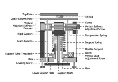
 Negative-stiffness mechanism (NSM) isolators have
the flexibility of custom tailoring resonant frequencies
vertically and horizontally. They employ a completely
mechanical concept in low-frequency vibration isolation.
Vertical-motion isolation is provided by a stiff spring
that supports a weight load, combined with a NSM. The
net vertical stiffness is made very low without affecting
the static load-supporting capability of the spring.
Beam-columns connected in series with the vertical-motion
isolator provide horizontal-motion isolation. The horizontal
stiffness of the beam-columns is reduced by the "beam-column"
effect. A beam-column behaves as a spring combined with
a NSM. The result is a compact passive isolator capable
of very low vertical and horizontal natural frequencies
and very high internal structural frequencies.
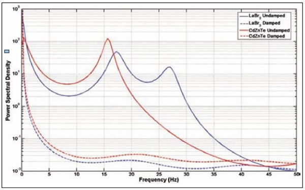
Vibration transmissibility with Negative-Stiffness is substantially improved over air systems, which can make vibration isolation problems worse since they have a resonant frequency that can match that of floor vibrations. Transmissibility is a measure of the vibrations that transmit through the isolator relative to the input vibrations. The NSM isolators, when adjusted to 0.5Hz, achieve 93 percent isolation efficiency at 2Hz; 99 percent at 5Hz; and 99.7 percent at 10Hz.

NSM transmissibility is also improved over active systems.
Because they run on electricity, active systems can be negatively
influenced by problems of electronic dysfunction and power
modulations, which can interrupt crystal growth continuity.
Active systems also have a limited dynamic range - which
is easy to exceed - causing the isolator to go into positive
feedback and generate noise underneath the equipment. Although
active isolation systems have fundamentally no resonance,
their transmissibility does not roll off as fast as Negative-Stiffness
isolators.
"One of the concerns we had was surface waves coming
across the ground, which induced vibration in the crystal
growth system," explains Harrison.
"We are located in a basement," Harrison says. "Before we got the NSM system, I could actually see somebody walking down the stairs through the walls with a seismometer. With the Negative-Stiffness system in place, I can't even tell when they are shelling at the nearby Fort Riley military base.

Improving Detection of Special Nuclear Materials
Gamma ray detectors have been around for years, but they
are either very low efficiency, poor performance or they
require liquid nitrogen cooling, such as those employing
germanium. Imagine the difficulty required to take liquid
nitrogen into a remote desert searching for special nuclear
material.
"What we are trying to do at SMART Lab is make it more
feasible, more economical for these detectors to be put
in place at every critical check point, at every airport
and shipping port," Harrison says. "This will
increase the possibility of detecting and intercepting shipments
of special nuclear material, should they occur."
About Kansas State University SMART Laboratory
The SMART Laboratory serves as a center for undergraduate
and graduate student education, as well as a facility, to
accommodate funded research projects from various government
and industrial sponsors. Since the opening of the Laboratory
in 1998, eleven patents have been awarded to SMART Laboratory
researchers for various detector designs, with several more
patents still pending.
The Laboratory's equipment includes an assortment of semiconductor
processing equipment, including a linear-drive diamond cutting
wheel, diamond wire saw, precision slurry saw, wafer dicing
saw, precision lapping and polishing machines, a custom
chemo-mechanical polishing system, a custom 6-pocket e-beam
evaporator, a 4-pocket evaporator, two dual filament evaporators,
an ion mill, vacuum annealing chamber, fission chamber plating
station, mask aligners, microscopes, ovens, grinders, and
an assortment of various furnaces for annealing, sintering,
diffusions and oxidations.
The Lab has numerous crystal growth furnaces used to grow
CdZnTe, LaBr3, and HgI2 crystals for radiation detector
development, which include 40 horizontal and 10 vertical
HgI2 vapor transport furnaces, two high pressure vertical
Bridgman furnaces, two low pressure vertical Bridgman furnaces,
three zone-melt furnaces, a vapor transport purifying furnace,
and a GaAs LPE furnace.
Central to SMART Laboratory is a Class-1000 cleanroom where
radiation detectors are fabricated. The Laboratory is equipped
with a scanning electron microscope, Auger electron analyzing
system, IV and CV tracers, ellipsometer, probers, radiation
sources and Nuclear Instrumentation Module (NIM) electronics
to test and characterize radiation detectors and materials.
About Mark J. Harrison
Mark J. Harrison, PhD, has a B.S. in mechanical engineering,
and an M.S. and PhD in nuclear engineering. Dr. Harrison
holds the position of assistant professor in the Nuclear
and Radiological Engineering Department at the University
of Florida, Gainesville, and participates in radiation detection
research at the Semiconductor Materials and Radiological
Technologies Laboratory (SMART Lab) at Kansas State University,
in collaboration with his colleague, Kansas State University
resident professor Douglas S. McGregor.
Professor Harrison can be reached by contacting the Nuclear
and Radiological Engineering Department, University of Florida;
202 Nuclear Science Bldg., Gainesville, FL 32611; Phone:
352-392-1401 ext. 317; Fax: 352-392-3380; email: mark.harrison@ufl.edu.
The SMART Laboratory is directed by Prof. Douglas McGregor,
who can be reached by contacting the Mechanical and Nuclear
Engineering Department, Kansas State University; 3002 Rathbone
Hall, Manhattan, KS 66506; Phone: 785-532-4093; Fax: 785-532-7057;
email: mcgregor@ksu.edu.
About Minus K Technology, Inc.
Minus K® Technology, Inc. was founded in 1993 to develop,
manufacture and market state-of-the-art vibration isolation
products based on the company's patented negative-stiffness-mechanism
technology. Minus K products are used in a broad spectrum
of applications including nanotechnology, biological sciences,
semiconductors, materials research, zero-g simulation of
spacecraft, and high-end audio. The company is an OEM supplier
to leading manufactures of scanning probe microscopes, micro-hardness
testers and other vibration-sensitive instruments and equipment.
Minus K customers include private companies and more than
200 leading universities and government laboratories in
35 countries.
Dr. David L. Platus is the inventor of negative-stiffness
mechanism vibration isolation systems, and President and
Founder of Minus K Technology, Inc. (www.minusk.com). He
earned a B.S. and a Ph.D. in Engineering from UCLA, and
a diploma from the Oak Ridge School of (Nuclear) Reactor
Technology. Prior to founding Minus K Technology he worked
in the nuclear, aerospace and defense industries conducting
and directing analysis and design projects in structural-mechanical
systems. He became an independent consultant in 1988. Dr.
Platus holds over 20 patents related to shock and vibration
isolation.
For more information on negative-stiffness vibration isolation
please contact Steve Varma, Minus K Technology, Inc.; 460
South Hindry Ave., Unit C, Inglewood, CA 90301; Phone 310-348-9656;
Fax 310-348-9638; email sales@minusk.com; www.minusk.com.