![]()
U.S. Tech – March 2022
Test and Measurement
Negative-Stiffness Vibration Isolation Aids Quantum Electronic Research
By Jim McMahon
Better understanding the character and properties of graphene, and similar two-dimensional materials, will advance their integration into improvements for semiconductors, electronics, photovoltaics, battery energy storage and many other applications.
One university laboratory that has been conducting research with graphene and other atomically-thin materials for some years is the Henriksen Research Group at Washington University in St. Louis, Missouri.
“Our experiments entail the careful measurement of the electronic properties of thinly-layered materials, including both electronic transport and thermodynamic quantities, such as the magnetization and compressibility of electron gas,” says Professor Erik Henriksen Ph.D., leading professor of the Henriksen Research Group. “We also conduct measurements of the infrared absorption spectrum to probe the electronic structure directly.”
The group searches for unusual and unexpected properties of low-dimensional materials, utilizing a combination of electronic, optical and thermodynamic measurement approaches to understand the novel quantum electronic phases that arise. The experiments are generally conducted at very low temperatures, fractions of a degree Kelvin above absolute zero, and in high magnetic fields, employing custom devices made of graphene or related crystals.
Single-Atom Flakes
“We look at the physics of the layered graphene, where the layers are weakly bound, so they can be pulled apart,” explains Henriksen. “We isolate these very thin layers down to a single atom. Then, lift the
graphene flakes from bulk graphite with adhesive tape, transferring them very carefully onto silicon wafers.”
Once on the silicon wafers, the exfoliated graphene flakes are encapsulated for protection, and transported to a cleanroom with a cryostat ultra-high vacuum chamber for AFM measurements, infrared spectrum absorption and related testing.
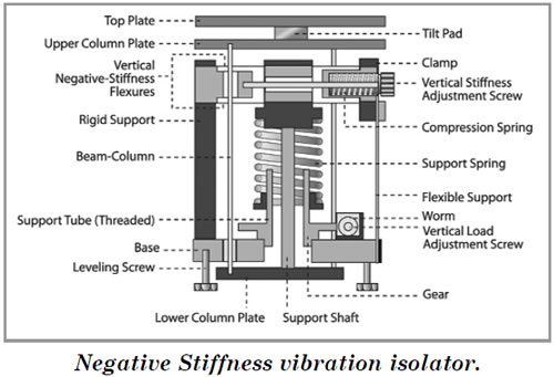
Manipulating these samples and positioning them on wafers, consequently, requires a stable platform for the atomic force microscope. For this purpose, the lab selected a Negative-Stiffness vibration isolation system.
Vibration Isolation
Negative-Stiffness vibration isolation was developed by Minus K Technology. These vibration isolators are compact, and do not require electricity or compressed air which enables sensitive instruments to be located wherever a production facility or laboratory needs to be located. There are no motors, pumps or chambers, and no maintenance because there is nothing to wear out. They operate purely in a passive mechanical mode.
What is very advantageous about Negative-Stiffness isolators is that they achieve a high level of isolation in multiple directions. Negative-Stiffness isolators deliver very high performance, as measured by a transmissibility curve. Vibration transmissibility is a measure of the vibrations that are transmitted through the isolator relative to the input vibrations.
Contact: Minus K Technology, Inc., 460 S. Hindry Avenue, Unit C, Inglewood, CA 90301, 310-348-9656 E-mail: request@minusk.com Web: www.minusk.com
|