|
|
Newsletter November 2020 | Menu of Newsletters

You might have thought, maybe for only a
few moments, that your audio system was sounding especially good. With that
feeling, you would have rated the sound a top score of "10". Then those magical
moments ended and your system returned to it's normal - but still good -
performance level. Well, folks, the Minus K
CT-2 Isolation
Platform could raise your system score to an "11" and keep it there! Highly
recommended for systems that are already high performance and where you want to
coax the maximum performance from your audio investment....
Dr. David L.
Platus is President and Founder and is the principal inventor of the
technology. He earned a B.S. and a Ph.D. in Engineering from UCLA, and a
diploma from the Oak Ridge School of (Nuclear) Reactor Technology. Prior to
founding Minus K® Technology he worked in the nuclear, aerospace and
defence industries conducting and directing analysis and design projects in
structural-mechanical systems. He became an independent consultant in 1988. Dr.
Platus holds over 20 patents related to shock and vibration
isolation.

Ultra-Thin 2.7" High CT-2 Product
Attributes:
- Isolation performance is typically 10 to 100 times
better than air systems
- No air or electric power is
required
- Nothing to wear out
- No
maintenance
A complete description of the
patented
Negative-stiffness design can be found on the
Technology page of the manufacturers Web site. The Minus K platform is
completely silent and requires no pumps or power. The
CT-2 model platforms
are available for different weight ranges of payload, or supported weight. The
40CT-2 model, while not specifically listed on the Web page, was perfect for
the Clearaudio Ovation turntable used for this review. The platform dimensions
are 18" W x 20" D x 2.7" H, with a weight of about 30 pounds. Different models,
for different payloads, range in price from $4,650 to about $5,250. In my
system, the platform was installed 20" W x 18" D, which placed the adjustment
crank on the 18" left side.
The horizontal frequency of ~1.5 Hz is
achieved at or near the upper limits of the payload range. The vertical
frequency is tunable to 0.5 Hz throughout the payload range. What this means is
that any very low frequency vibrations that are not blocked or absorbed by the
Minus K platform are several orders of magnitude below what your phono
cartridge, or even the best subwoofers, can process.
Full article...
|
|

Technology is winner of a Laser Focus World Innovator
Award
CT-2 Ultra-Thin Low-Height
Tabletop Vibration Isolation Platform
 The Compact Tabletop (CT-2)
uses Minus K's patented breakthrough technology allowing for the best
performance on the market in just a 2.5 inch tall isolation platform. This unit
is an upgrade from Minus K's CT-1 and offers better horizontal performance with
additional payload ranges for heavier instruments.
This is the
thinnest, most portable and most user-friendly isolator ever offered that
is capable of delivering this performance.more...:
- Horizontal frequencies are weight dependent.
- Horizontal frequency of ~1.25 Hz is achieved at or near the upper
limits of the payload range.
- At the lower payload weights the horizontal frequency will
increase.
- Vertical frequency is tunable to 0.5 Hz throughout the payload
range.
Pricing & sizes for
CT-2
Press Release for the
CT-2
|

3D Surface Analysis Vibration
Isolation
High-precision, nanometer-level 3D surface
measurement systems can be negatively affected by low-frequency
vibration—distorting imaging and producing inaccurate measurement
readings. |
Manufacturers need to control processes to
produce a consistent, reliable product. Where precision surface engineering is
required, surface measurement may be a key part of maintaining control of the
process, by checking output to see that the process is not outside of
specification.
3D non-contact surface analysis is widely used in the
industry for the measurement of small displacements and surface irregularities.
It delivers the ultimate in high accuracy and repeatable and traceable
measurement. When built into microscopy equipment, employing 3D laser scanning
or structured light, these systems report the surface condition of a product
with more accuracy than any other methodproviding nanometer-level profile
measurements of height, width, angle, radius, volume, and roughness. Such
precision measurement systems allow users to improve product quality and
reliability, and increase manufacturing consistency and production
yields.
Low-Frequency Vibration
When measuring at such high
levels of precision, any instrument can be negatively affected by low-frequency
vibrations generated within a manufacturing facility. These can distort
measurements and impact imaging and measurement data
One company that
has great familiarity with the manufacturing environment and 3D surface
measurements is Keyence Corporation--a leading supplier of sensors, measuring
systems, laser markers, microscopes, and machine vision systems
worldwide.
We have many customers with high-precision 3D measurement
systems operating in high-vibration environments, performing microscopy
evaluation at 30,000 times magnification, looking at nanometer-level surface
features, said Evan Eltinge, Senior Sales Engineer Surface Analysis Team, with
Keyence Corporation of America. At that level of detail, and in that
environment, if measures are taken to reduce vibration it improves the quality
of the data.
Without proper isolation surface measurements occurring at
3,000 to 5,000 times magnification, the vibration could contribute to image
blurring and loss of image quality, continued Eltinge.
Vibration can be
caused by a multitude of factors within a plant; every structure is
transmitting noise. Within the building itself, production machinery, forklift
trucks, the heating and ventilation system, fans, pumps, compressors, and
elevators are just some of the mechanical devices and equipment that create
low-frequency vibration. Depending on how far away the surface measurement
instrumentation is from these vibration sources, and where inside the structure
the instrumentation is locatedwhether on the production floor or in a loftwill
determine how strongly the instrumentation will be influenced.
External
to the building, the equipment can be influenced by vibrations from truck
movement, road traffic, nearby construction, loud noise from aircraft, and even
wind and other weather conditions that can cause movement of the
structure.
Vibration Isolation Options for 3D Surface
Analysis...
Full article...
|

The Moulé Group, at the University
of California/Davis, is interested in the solution processing and patterning of
organic electronic materials for use in devices such as light-emitting diodes,
photovoltaics, transistors, thermoelectric, and chemical sensors. The Group
specifically focuses on using structural and dynamic measurement techniques to
quantify the effects of solution processing and patterning on material
morphology and device architecture.
Tucker Murrey, a doctoral candidate
and published author with the Moulé Group, is actively involved with
researching and designing a scalable optical patterning process for organic
photovoltaic applications.
"Most working organic devices consist of
several layers of material, each having a specific optical and/or electronic
function," said Murrey. "One universal design constraint for complicated device
architectures, like organic field-effect transistors (OFETs), organic
photovoltaics (OPVs) and red-green-blue organic light-emitting diode (OLED)
displays is that they require multiple components patterned laterally and
vertically to operate. Currently, many of these components are comprised of
non-flexible inorganic materials. In order to move towards flexible, all
organic electronic devices, there is a need to develop high precision vertical
and lateral patterning methods that are compatible with solution processing.
mmense efforts in the plastic electronics field have led to
unprecedented progress and continuous improvements in organic photovoltaic
(OPV) performance.
"Given that conventional photolithography technology
techniques are incompatible with polymeric semiconductors, there is a critical
need to develop scalable photopatterning methods capable of laterally
patterning organic semiconducting compounds with sub-micromometer resolution,"
added Murrey. "This patterning process would enable the construction of a
sophisticated OPV architecture designed to increase external quantum
efficiency."
"A scalable process for controlling film topography with
sub-micrometer resolution would represent a substantial development that
enables the advancement of complex organic electronic device architectures,"
continued Murrey.
Photothermal Projection Lithography
The
Moulé Group is working on a series of solution-based methods, one of
which is called Photothermal Projection Lithography for Polymeric
Semiconductors with Sub-diffraction Limited Resolution.
Polymeric
semiconductors combine many of the electrical properties of inorganic
semiconductors with the mechanical flexibility and chemical processability of
organic materials, such as enabling them to be deposited from solution over
large areas, greatly reducing production costs compared to conventional
metallic semiconductors. Developments like this have motivated a rapid increase
in demand for low-cost, high-throughput, and high-resolution fabrication
techniques.
Organic semiconductors are non-metallic materials that
exhibit semiconductor properties, whose building blocks are polymers made up of
carbon and hydrogen atoms. These conductive polymers are, essentially,
electrical insulators, but become conducting when charges are either injected
from electrodes or by photoexcitation, or doping the intentional introduction
of impurities into an intrinsic semiconductor for the purpose of modulating its
electrical, optical, and structural properties.
"Over the past year I
have been upscaling an optical patterning process that our group developed to
make micro-scale electronic devices with these materials," expressed Murrey.
"The overall pattern area was limited to less than one square millimeter. Now
we are trying to upscale the overall patterning area to about one square
centimeter."
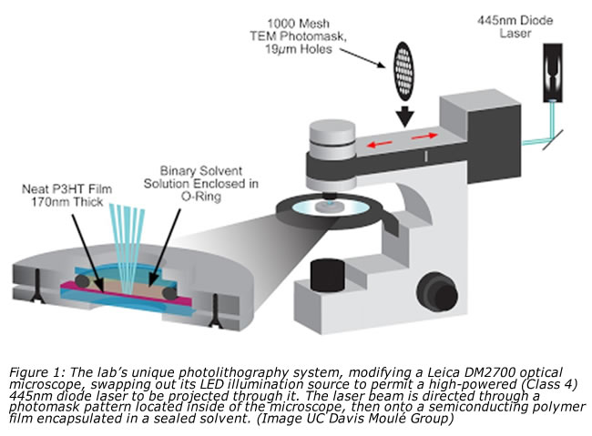
Murrey designed a unique lab-scale photolithography system,
modifying a Leica DM2700 optical microscope, swapping out its LED illumination
source to permit a high-powered (Class 4) 405nm diode laser to be projected
through it. Built into the system is a laser beam expander, collimating lens,
and an optical speckle remover.
 |
Full article...
|
 |
|
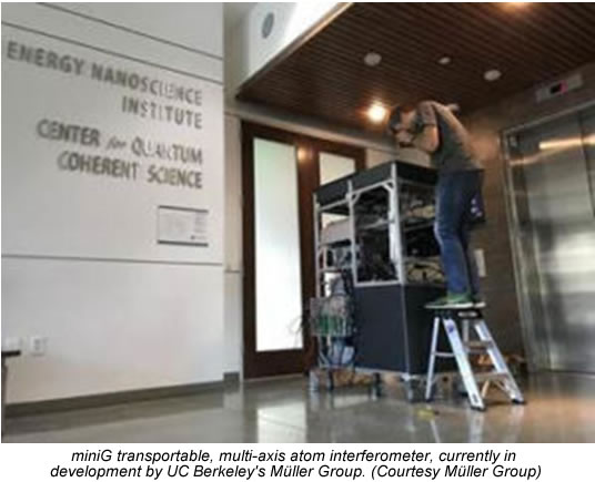
Professor Holger Müller's Group at UC
Berkeley is focused on advancing experimental quantum technology to push the
sensitivity of experiments to new levels, and to perform precision measurements
of fundamental constants. The groups work uses methods from atomic, molecular
and optical physics. One project is the development of a transportable,
multi-axis atom interferometer, named miniG.
MiniG was designed to
research how quantum interference can be used to measure gravity outside of the
laboratory. When cooled to just above absolute zero, the atoms form the focus
of a portable quantum gravimeter.
Gravimeters, used to measure
gravitational acceleration, have been successfully applied for metrology,
geology and geophysics. MiniG uses an atom interferometer to measure the effect
of gravity on clouds of atoms that are first trapped and cooled. Interferometry
inherently depends on the wave nature of the object. Particles, including
atoms, can behave like waves. Atom interferometers measure the difference in
phase between atomic matter waves along different paths.
We use atoms
that are laser-cooled to millionths of a degree above absolute zero, said
Xuejian Wu, a post-doctoral scholar, involved in the development of miniG at
the Müller Group. With pulses of light, we drive each atom into a quantum
superposition of having been kicked with the momentum of photons, or not
kicked. The atoms, in two places at one time, are in a superposition of
recoiling backwards or staying still. By manipulating the state of the atoms
using one of two types of such light pulses, we steer the matter waves' paths
and recombine the matter waves at the end of the experiment.
Atom
interferometry has become one of the most powerful technologies for precision
measurements, and atomic gravimeters, based on atom interferometry, are
extremely accurate and have long-term stability.
Current atom
interferometers, however, are too complicated to operate in a miniature package
or under field conditions. Berkeleys mini-G was engineered to resolve this
issue.
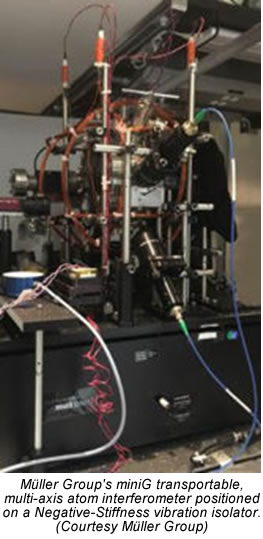
In this project, we are developing a mobile atom interferometer
using a single-diode laser system and a pyramidal magneto-optical trap,
continued Wu. This allows the device to be smaller, simpler and more robust
than conventional atom interferometers.
Vibration
Isolation

Measurements of atomic precision require
isolation from ambient vibrations coming from internal and external sources. As
measurements are being done at a smaller and smaller level, those vibrations
that are present will start to dominate, and the need for more effective
isolation increases.
Although the Müller Groups research
laboratory is situated in the basement of a building on the Berkeley campus, it
is still influenced by vibrations from the buildings HVAC system.
For
several years now we have been using
Negative-Stiffness vibration isolation for our
research projects, continued Wu.
Full article...
|
|
|

 |
|
|
