|

Combining Laser Scanning and Spectroscopy for Enhanced
Nanolithography Patterning

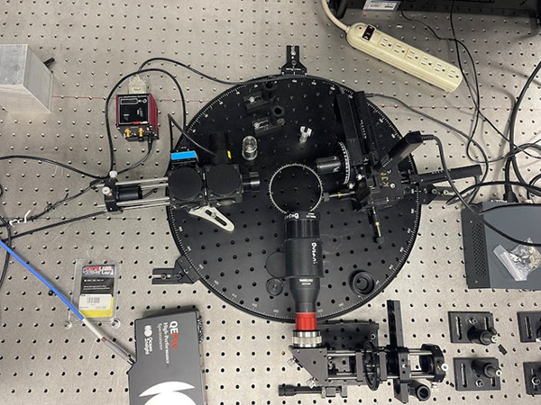
The Busani
Research Group’s AFM probe for semiconductor patterning, equipped with an
aluminum nitrate laser nanowire used as a lithographic tip, allows traditional
laser scanning to be performed along with spectroscopy to record the
fluorescence signal of the material. Using Minus K Vibration
Isolators.
Scanning probe microscopy
(SPM) constitutes a family of advanced techniques for surface analysis. The
current progress in SPM of polymers, metals, semiconductive, and insulating
materials largely stems from the development of atomic force microscopy (AFM).
AFM is recognized as a powerful device for obtaining information of material
surface structures at the nanoscale. It is used for measuring not only
inorganic materials such as metals and semiconductors, but also organic
materials and biomaterials.
AFM patterning and imaging techniques are
used widely to conduct research into nanoscale device fabrication. In AFM, the
sample surface is scanned with a probe consisting of a miniature cantilever and
a sharp tip. The tip apex is in continuous contact with the surface when
imaging is performed in AFM contact mode, or it is in intermittent contact with
the sample in the tapping mode. However, imaging by AFM of high-aspect-ratio
nanostructures with sharp edges and straight walls in nanoscale metrology is
challenging due to the mechanical properties and conical geometry of most
commercially available tips.
Nanowires enhance AFM probe
functionality
One-dimensional (1D) semiconductor nanostructuressuch as
nanowires and nanotubes, commonly defined as linear structures with a diameter
less than 100 nmhave emerged as building blocks for the next generation of
electronic and optoelectronic nanodevices because of their unique physical and
chemical properties
Gallium nitride (GaN) nanowires are embedded into
probes for nanoscale metrology of high-aspect-ratio structures to enhance the
resolution of AFM imaging. They also permit combining AFM with other tools such
as scanning tunneling microscopy (STM) and near-field scanning optical
microscopy (NSOM) to produce a universal multipurpose probe. This combination
can be used to enhance lithography and microscopy
techniques.
Vibration isolation
Since Busanis group deals with
nanostructures, ground vibration is important. We needed an antivibration
system for two reasons: for our laser optics, and for our AFM system that we
integrate with an external laser source, Busani says. The sample that gets
exposed to the laser beam on the AFM needs to be optically stable.
Full
article...
|
