![]()
U.S. Tech - March 2025
ELECTRONIC MFG. SERVICES (EMS)
Phonon Momenta Mapping at Atomic Resolution
Technological advancement has been successful in miniaturizing components and structures in electronics to such a degree that they are on the order of a billionth of a meter. Central to engineering these nano-components is understanding the properties of phonons.
Mapping phonons, a quantum of energy quasiparticle associated with a compressional wave, in nanostructures is indispensable to the development and understanding of thermal nanodevices, modulation of thermal transport, and novel nanostructured thermoelectric materials. In crystals, which hold an ordered atomic structure, these phonon waves of atomic dis- placements tend to carry thermal energy equal to their frequency of vibration.
Through the engineering of complex structures such as alloys, nanostructures and superlattice interfaces, it is possible to alter their thermal conductivity by controlling the propagation of phonons while maintaining electrical conductivity. To achieve high phonon impedance it is optimal for nanostructures to have an abrupt change in structure which lowers their conductivity.
Studying Phonon Behavior
Utilizing an alloy of germanium and silicon, a research team consisting of UCI's IMRI, the Massachusetts Institute of Technology (MIT), and other institutions, was capable of studying how phonons tend to behave in the disordered surrounding of the quantum dot - the interface between the quantum dot and the encircling silicon, and next to the dome-shaped surface of the quantum dot nanostructure itself. Quantum dots are semiconductor particles a few nanometers in size with optical and electronic properties that differ from those of larger particles via quantum mechanical effects. They are a central topic in nanotechnology and materials science.
With the help of a Nion UltraSTEM 200 scanning transmission electron microscope (STEM), the research team has developed a novel technique to map phonons in crystal lattices at atomic resolution. To examine how phonons are dis-tributed by the interfaces of Si/SiGe (silicon-germanium heterostructure) quantum dots, the team probed the dynamic behavior of phonons next to a single quantum dot of silicon-germanium utilizing vibrational electron energy loss spectroscopy (EELS) in the STEM at IMRI. EELS is a technique that measures the bonding environment of molecules with high spatial resolution.
 "We developed a novel technique to differentially map phonon momenta with atomic resolution, which enables us to observe non- equilibrium phonons that only exist near the interface," says Dr. Xiaoqing Pan, UCI professor of materials science and engineering, and physics, Henry Samueli Endowed Chair in Engineering, and IMRI Director.
This research has allowed a deeper knowledge of the way heat tends to travel via quantum dots and engineered nanostructures in electronic components. At the atomic scale, heat is transported in solid materials as a wave of atoms that have been moved from their equilibrium position as heat shifts away from the thermal source.
"This work marks a major advance in the field because it is the first time we have been able to pro- vide direct evidence that the inter- play between diffusive and specular reflection largely depends on the detailed atomistic structure," adds professor Pan.
Isolating Vibrations
UC Irvine set out to build a world-class electron microscopy facility to house the most sensitive transmission electron microscopes (TEMs) available, and to accommodate next-generation instruments expected in the coming decades. To this end, in 2015 existing ground floor engineering classrooms were converted, establishing the IMRI within the UCI Samueli School of Engineering.
To mitigate noise and vibration impacts, each instrument room slab was physically isolated from the existing building structural elements and from new, adjacent walls.
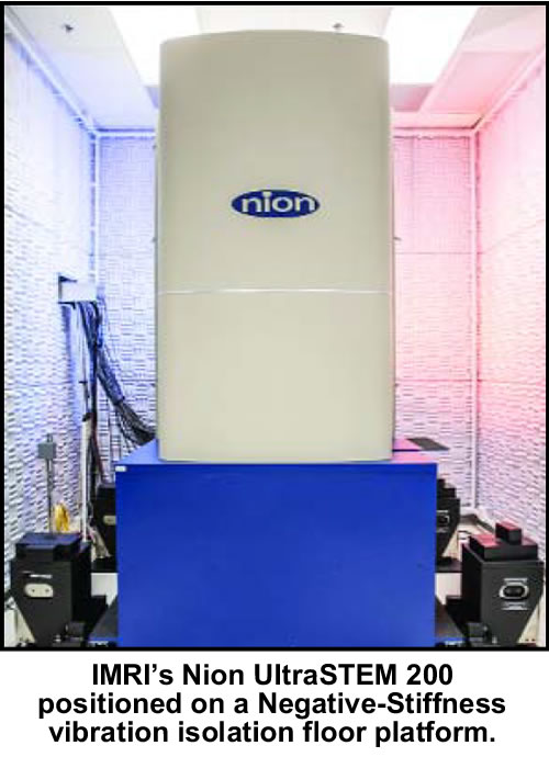
At IMRI's STEM-1 room, a custom vibration isolation platform was installed to further reduce vibrations experienced by the lab's Nion UltraSTEM 200 to produce distortion free imaging at magnifications as small as sub-angstrom levels - smaller than the width of an atom. Additional preparation for the Nion UltraSTEM included recessing of the vibration isolation platform so the front section of the Nion could be rolled off and on, and the instrument could be accessed and serviced when not imaging. IMRI selected a Negative-Stiffness vibration isolation platform from Minus K Technology (Minus K) for its Nion UltraSTEM 200.
Negative-Stiffness vibration isolators are compact and do not require electricity or compressed air, there are no motors, pumps, or chambers, and no maintenance because there is nothing to wear out. They operate purely in a passive mechanical mode.
"Vertical-motion isolation is provided by a stiff spring that sup- ports a weight load, combined with a negative-stiffness mechanism," says Erik Runge, vice president of engineering for Minus K. "The net vertical stiffness is made very low without affecting the static load- supporting capability of the spring. Beam-columns connected in series with the vertical-motion isolator provide horizontal-motion isolation. The beam-columns behave as a spring combined with a negative- stiffness mechanism. The result is a compact passive isolator capable of very low vertical and horizontal natural frequencies and high internal structural frequencies."
The isolators achieve a high level of isolation in multiple directions and offer the flexibility of custom tailoring resonant frequencies to 0.5 Hz vertically and horizontally. For an isolation system with a 0.5 Hz natural frequency, isolation begins at 0.7 Hz and improves with increases in the vibration frequency. The natural frequency is more commonly used to describe the system performance.
Negative-stiffness isolators deliver high performance as measured by a transmissibility curve. Vibration transmissibility is a measure of the vibrations that are transmitted through the isolator relative to the input vibrations. Negative-stiffness isolators, when adjusted to 0.5 Hz, achieve approximately 93 percent isolation efficiency at 2 Hz, 99 percent at 5 Hz, and 99.7 percent at 10 Hz.
Research Outcome
One of the main results of IMRI's research is the development of a new method for mapping the direction of thermal carriers in materials.
"This is analogous to counting how many phonons are going up or down and taking the difference, indicating their dominant direction of propagation," explains Dr. Pan. "This technique allowed us to map the reflection of phonons from interfaces."
Contact: Minus K Technology, Inc., 460 Hindry Avenue, Unit C, Inglewood, CA 90301, 310-348-9656 E-mail: sales@minusk.com Web: www.minusk.com
|